Table of contents
- Helpful webpages:
- Link to inclusion in public webpage:
- Slides PDF:
- Speaker notes:
- Introduction slide / General speaker notes
- Slide 1: The photoelectric effect
- Slide 2: Quantum tunneling
- Slide 3: Transistors
- Slide 4: Moore’s law
- Slide 5: Electronic behavior in nanomaterials
- Initial Notes
Helpful webpages:
https://physics.illinois.edu/people/directory/profile/nadya
Link to inclusion in public webpage:
Slides PDF:
Speaker notes:
Introduction slide / General speaker notes
Researcher's background:
Mason completed her bachelor’s degree in physics at Harvard University, graduating in 1995. She received her doctorate in physics from Stanford University in 2001, where she wrote her thesis on phase transitions in two-dimensional superconductors under the supervision of Aharon Kapitulnik. She was a Junior Fellow at the Harvard Society of Fellows where she researched carbon nanotubes and nanostructured superconductors. She became a John Bardeen Faculty Scholar in Physics at the University of Illinois at Urbana-Champaign in 2014 and was appointed full Professor in 2016. She is the Director of the Illinois Materials Research Science and Engineering Center, a General Councillor for the American Physical Society, Chair of APS Committee on Minorities and was featured by the National Society of Black Physicists for Black History Month in 2017. Her awards include, but are not limited to, election to the American Academy of Arts and Sciences and the to the US National Academy of Sciences (2021), the Edward Bouchet Award from the American Physical Society (2020), the Dean’s Award for Excellence in Research from the University of Illinois at Urbana-Champaign (2013), and the Maria Goeppert Mayer Award from the American Physical Society (2012).
Synopsis of Work:
Nadya Mason is a condensed matter experimental physicist who researches the electronic properties of nanomaterials such as graphene, carbon nanotubes, topological insulators, nanostructured superconductors, and other low-dimensional systems. These materials have applications for quantum computing because they can act like switches in the way that transistors do, but without the limitations on transistors’ physical sizes due to quantum tunneling. Mason conducts tunneling experiments on carbon nanotubes and studies nanostructured superconductors. Her work explores the properties of materials that will make up the next generation of technology.
Citations and resources:
https://www.aps.org/careers/physicists/profiles/mason.cfm
https://mrl.illinois.edu/directory/profile/nadya
https://en.wikipedia.org/wiki/Nadya_Mason
Societal relevance of work:
Transistors are semiconducting devices that make up the circuitry in modern electronics. They are smaller than 50 nm and are continuing to get smaller with technological developments. There is a limit, however, to how small a transistor can be made due to quantum mechanical effects. Transistors act like switches because they contain a gap where electrons don’t flow until an external voltage is applied. Because of particle-wave duality, electrons are able to tunnel through potential barriers at very small scales, meaning transistors cannot continue to get smaller and still function. To keep up with the need for smaller components of modern circuits, scientists are researching new materials to use in electronic devices. These devices include graphene, carbon nanotubes, topological systems, and semiconducting nanowires. These are low-dimensional systems wherein electrons display quantum properties and have novel effects which Mason seeks to uncover. Her research has applications for quantum communication, information storage, and qubit control for quantum computing.
Slide 1: The photoelectric effect
Science details:
Quantum mechanics is a fundamental theory that describes nature at the smallest scales. Classical theories of physics are not able to completely explain the interactions of matter and energy at the atomic and subatomic scales. Max Planck theorized that electromagnetic energy is not continuous but rather comes in packets (photons) with discrete (quantized) energies. The energy of a single photon of frequency ν is given by E=hν, where h is Plack’s constant. In the 19th century, light was generally believed to be described entirely by wave theory, which explained observations of refraction, diffraction, interference, and polarization. The photoelectric effect, however, could not be explained in terms of waves alone but suggested that light has a particle-like nature.
The photoelectric effect is the emission of electrons by a material in response to light or other electromagnetic radiation being shone on it. Classical electromagnetism predicts that when continuous electromagnetic energy is transferred to electrons, they are emitted when they accumulate enough energy and increasing the intensity of light should change the kinetic energy of the emitted electrons. Experimentally, however, electrons are only emitted if the light has a high enough frequency and the intensity of light does not have an effect on the kinetic energies of the emitted electrons. This is because a beam of light can be described as a stream of photons, with energies proportional to the light’s frequency which determine the ejection energies. The photoelectric effect demonstrated the quantum nature of light.
Citations and resources:
https://en.wikipedia.org/wiki/Introduction_to_quantum_mechanics#The_photoelectric_effect
http://hyperphysics.phy-astr.gsu.edu/hbase/mod1.html
https://en.wikipedia.org/wiki/Photoelectric_effect
Figures:
Schematic of the photoelectric effect. The energy of a photon is given by E_photon=hν. Photons of different wavelengths are shown striking a sheet of potassium which requires 2.0 eV to emit an electron. The red photon has a wavelength of 700 nm and energy of 1.77 eV and no electrons are emitted. The green photon has a wavelength of 550 nm and energy of 2.25 eV causing an electron to be emitted with maximum frequency of 2.96✕10⁵ m/s. The purple photon has a wavelength of 400 nm and energy of 3.1 eV causing an electron to be emitted with maximum frequency of 6.22✕10⁵ m/s. http://hyperphysics.phy-astr.gsu.edu/hbase/mod1.html
Slide 2: Quantum tunneling
Science details:
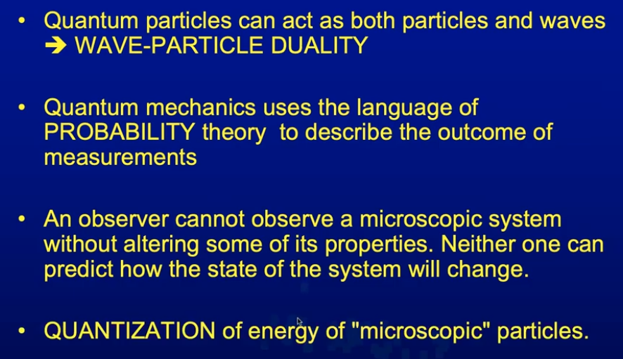
Quantum tunneling is a quantum mechanical phenomenon wherein a particle can be transmitted through a potential barrier. In classical physics the particle would be repelled if its energy is less than that of the barrier. In quantum mechanics, particles can be understood using the language of probability theory because they have wave properties and are mathematically described by wavefunctions. This implies that a particle’s position and momentum cannot be simultaneously measured to a particular position (given by the Heisenberg uncertainty principle), meaning the particle has a non-zero probability of being on the other side of the barrier. As the energy of the potential barrier increases, the probability of the particle tunneling through it decreases.
Citations and resources:
https://en.wikipedia.org/wiki/Quantum_tunnelling
Figures:
Top: Classical picture of a particle (electron) striking a barrier (electric field) and being repelled by it.
Bottom: Quantum picture of an electron wave approaching a barrier and tunneling through it.
http://abyss.uoregon.edu/~js/glossary/quantum_tunneling.html
Slide 3: Transistors
Science details:
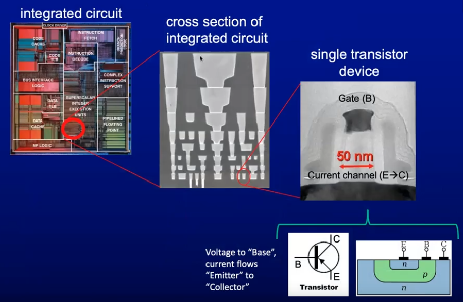
Transistors are semiconducting devices that are used in the circuitry of modern electronic devices. Modern transistors are smaller than 50 nm, and a single CPU can contain billions of transistors. They are solid state devices that can be used to amplify signals or act like on/off switches. In the absence of an applied voltage there is no current that flows across the gap, but current will flow when triggered by an external voltage.
Transistors are made from silicon (a semiconductor) which is doped with different types of materials to control the flow of electrons and increase its conductivity. If silicon is doped with arsenic, phosphorus, or antimony, free electrons will flow more easily out of the silicon, which makes it an n-type (negative type) silicon. If it is doped with impurities such as boron, gallium, and aluminum then the free electrons will flow more easily into the silicon, making a p-type (positive type) silicon. P- and n- type silicons can be joined in various ways to create junction transistors which are turned on when the “holes” (absence of electrons) in the p-type and the surplus electrons in the n-type move across the junctions between the types. Quantum mechanics places a lower limit on the physical size of transistors: if the junction is too small then electrons can tunnel through, meaning the transistor will turn on without applying an external voltage.
Citations and resources:
https://en.wikipedia.org/wiki/Transistor
https://www.pcmag.com/encyclopedia/term/transistor
https://www.explainthatstuff.com/howtransistorswork.html
https://www.youtube.com/watch?v=w0Ce1tuW8nI
Figures:
Top left: Image of a transistor. https://www.istockphoto.com/photo/black-power-transistors-gm646291934-117194463
Top right: Schematic of a NPN junction transistor. A p-type base (red) is sandwiched between two n-type emitters (blue). https://learn.sparkfun.com/tutorials/transistors/all
Bottom right: Schematic of a field-effect transistor in its off and on states. Source and drain (metal) are shown in black, oxide is shown in blue, semiconductor made of p-type and n-type silicon is shown in light and dark orange, respectively. In the off state, the p-type silicon is shown with positive charges (electron holes) and the n-type silicon is shown with negative charges (excess electrons). The extra electrons between the source and the drain are not allowed to flow because of the holes in the gate between them. In the on state, a positive voltage is attached to the gate which allows electrons to flow from the source to the drain. GIF made using images from https://www.explainthatstuff.com/howtransistorswork.html
Slide 4: Moore’s law
Science details:
Moore’s law explains that the number of transistors in a single computer chip are increasing and the size of transistors are decreasing every year. There is a limit, however, to how small transistors can be made which is due to quantum mechanics: if the gap where current does not flow in the transistor’s off state is small enough (less than 5 nm) then electrons can tunnel through without an external voltage. Mason researches nanodevices that may provide a solution to the physical limit on the size of transistors as well as offer applications for quantum computers. These nanodevices include graphene (a single layer of atomic carbon), carbon nanotubes (rolled-up graphene), semiconductor nanowires, and topological systems (conducting surfaces with insulating bulks).
Citations and resources:
https://en.wikipedia.org/wiki/Quantum_tunnelling
https://phys.org/news/2009-11-superconducting-probes-picture-cnts.html
https://www.youtube.com/watch?v=tqb_zb0uBzM
Figures:
Top right: Moore’s law is shown by plotting the size of transistors in microns (left y-axis) and transistor count (right y-axis) against time, spanning from 1970 to 2020. The CPU transistor count doubles every 2 years, the feature size decreases by a factor of 0.7 every 2 years. https://www.researchgate.net/figure/Evolution-and-forecast-of-the-transistor-count-on-a-single-chip-according-to-Moores-Law_fig2_283906716
Bottom left: Illustration of graphene (left) and a carbon nanotube (right). https://www.nanotrun.com/article/talk-about-the-past-and-present-life-of-carbon-nanotubes-and-graphene-i00356i1.html
Bottom right: 3D illustration of a nanowire transistor. The drain (top) and source (bottom) are shown in green, the dielectric gate is shown in red, and the gate is shown in orange. https://www.fz-juelich.de/pgi/pgi-9/EN/Forschung-alt/01-Nanowires/_node.html
Slide 5: Electronic behavior in nanomaterials
Science details:
Mason conducts experiments by measuring the conductance and resistance of nanomaterials using nanodevices. Classically the resistance of a circuit follows Ohm’s law (resistance ✕ current = applied voltage), but quantum resistance is dependent on the properties of waves. In very small devices, such as quantum dots (nanoscale semiconductor particles that have quantum properties), Coulomb blockades can be observed. These are due to electrons inside the nanodevice repelling other electrons and blocking the current. This means that the nanodevice has a current-voltage relationship that does not follow Ohm’s law.
Carbon nanotubes, for example, have single electron conductance evidenced by quantized conductance peaks (which have heights equal to single electron energies) when measured against an electric field. Carbon nanotubes can also be used to show electron waves interfering by measuring the currents and applied electric fields: interference patterns (Fabry-Perot oscillations) emerge due to the wavelike properties of electrons bouncing within the nanotube. Mason has innovated techniques (such as superconducting tunneling spectroscopy) to study electrical conduction in carbon nanotubes, graphene, and other low-dimensional nanomaterials.
Citations and resources:
https://www.youtube.com/watch?v=tqb_zb0uBzM
https://en.wikipedia.org/wiki/Coulomb_blockade
https://en.wikipedia.org/wiki/Quantum_dot
https://www.nsf.gov/awardsearch/showAward?AWD_ID=0644674
Figures:
Top right: Plot of Coulomb blockade oscillations in a single-electron transistor. Current (in pA) is plotted against gate-source voltage V_GS (in mV). https://www.google.com/url?sa=t&rct=j&q=&esrc=s&source=web&cd=&ved=2ahUKEwiV88qitcb3AhVyhIkEHcdRDFMQFnoECCcQAQ&url=https%3A%2F%2Fwww.fkf.mpg.de%2F5694184%2FTutorial_SET2003.pdf&usg=AOvVaw3YN2L8k0EMnOBDaQJrRGvP
Middle: 3D illustration of a quantum dot. Gates 1 and 2 are down in brown, the coaxial nanowire is shown in green (center) and white (outer). The quantum dot is shown in red with spin pointing up. https://www.fz-juelich.de/pgi/pgi-9/EN/Forschung-alt/01-Nanowires/_node.html
Bottom left: Color plot of the differential change in current with respect to voltage (in e²/h) in a topological system. The y-axis is source-drain bias voltage V (in mV) and the x-axis is back gate bias voltage V_BG (in V). The diamond-shaped structures in the center are interference patterns which indicate low energy resonances. https://www.google.com/url?sa=i&url=https%3A%2F%2Farxiv.org%2Fpdf%2F1403.5588&psig=AOvVaw1MAQoFsvS2mR2Uk9_tpl1P&ust=1651708513682000&source=images&cd=vfe&ved=0CA0QjhxqFwoTCLj28e_DxPcCFQAAAAAdAAAAABAD
Initial Notes
- Lecture: Prof. Nadya Mason presents "Going through the quantum tunnel...". https://www.youtube.com/watch?v=tqb_zb0uBzM
- Condensed matter experimentalist focusing on electron behaviour in low-dimensional materials (nanowires, graphene, …). She also tries to increase diversity in materials sciences.
- Talk is divided into QM basics, then quantum electronic devices with examples from her work.
- QM intro: nature at smallest scales. Max Planck: EM energy is not continuous, packets=quanta of E=hf. Einstein: light is made of particles (photons) of energy E=hf (photoelectric effect slide?) and light is a wave. Particles are localized, waves propagate in space and interfere - superposition. DeBroglie: particle-wave duality. Particles as waves ⇒particles don’t have just one property (energy, momentum) so need language of probability theory. Entangled particles share properties when separated.
- 1st and last point are “most relevant for measuring solid state quantum devices”.
- Quantum for electronic devices? Electrons flow (tiny charged particles flow, classically), Ohm’s law. Electrons are also waves (confirmed by interference and diffraction experiments). Wave properties of electrons matter most when devices are very small.
- Can talk about band structure and how QM works into that?
- Electron wavelength around 1 nm (person wavelength around 1e-36 m). Nanoelectronics. Big electronics are run by little electrons (a microprocessor contains billions of transistors). Moore’s law: transistor size halves every 18 months.
- QM prevents us from fully turning off a transistor that is too small. Gates - closed, add voltage and it opens. Electrons go through a classical barrier (quantum tunneling) - happens around 5 nm. So QM limits shrinking of electronics because of (1) quantum tunneling (current flows without a voltage), (2) can’t turn current off at low power because of this gate insulator, (3) can’t run at high power without overheating.
- Need new nanomaterials with better properties (ultrasmall, low power dissipation, high sensitivity to gate voltage, novel effects): nanotubes, nanowires, topological systems, graphene.
- Studying nanomaterials: how well do they conduct electrons and resistance to electron flow. Classically: get Ohm’s law, quantum shows other stuff. Measuring quantum effects not super doable at room temp (get thermal effects) so need to cool to ~1 K or 15 mK.
- Eg: carbon nanotube, measure conductance (vs temp/B field/size) of a small section. See peaks (not Ohm’s law anymore - not linear) = quantized conductance peaks from single electrons tunneling on and off the nanotube.

- Also see interference: electrons in conductor and measure conductance - get interference pattern. (Fabry-Perot oscillations).

- Topological insulators: hollow wires, electrons go along outside - measure conductance vs. B field and see oscillations from constructive/destructive interference = shows surface states with little dissipation.
- Saturday Physics for Everyone 2017 https://www.youtube.com/watch?v=w0Ce1tuW8nI
- How do we study electronics? Measure resistance/conductance using a sensor.
- Transistors have semiconductors, ends have excess of electrons and middle has gap - no current flows through there. Apply a small current then get enough currents in middle then lots of electrons can flow. So they’re switches, solid state material. They can be very small. Modern ones are smaller than 50 nm.
- Solutions to QM limiting the size of transistors: use different materials and techniques (nanotubes, nanowires, graphene) that are ultrasmall, low power dissipation, high sensitivity to gate voltage, novel effects.
- Eg graphene: 1 atomic layer of carbon. (2010 Nobel prize using scotch tape). Measure its resistance. Made a super-fast transistor using graphene (low power dissipation, very fast) in 2011 or smt. Graphene isn’t nanoscale laterally so it’s good for layering - mechanical stability stuff, good for flexible electronics (wearable, integrated with clothing, sensors on bodies).

- She did tests stretching and straining graphene.
- How to improve computing w/o scaling down: quantum computers. Qubits do computations faster than classical bits.